Varistor image guide: types, symbols, and circuit diagram examples explained
Published Time:
2026-09-14
Author:
SUPfuse
Article overview
This guide covers the complete visual landscape of varistor image documentation — from schematic symbols and annotated physical photos to failure analysis and thermal imaging. It is written for electronics engineers and students who need accurate, multi-angle visual references to identify, specify, and troubleshoot metal oxide varistors in real circuits.
Table of contents
- 1. What is a varistor image and why does it matter
- 2. Varistor circuit symbols: IEC vs ANSI/IEEE explained
- 3. Physical identification: how to read markings on a real component
- 4. Side-by-side comparison of MOV, SiC, and ZnO varistor types
- 5. Real-world failure images: identifying damaged or burnt varistors
- 6. PCB placement images: SMD vs through-hole best practices
- 7. Thermal behavior during surge events
- 8. FAQ
What is a varistor image and why does it matter
A varistor image is any visual representation — photograph, schematic symbol, diagram, or annotated illustration — used to identify, document, or explain the appearance, structure, and electrical behavior of a varistor component. These visuals appear in datasheets, textbooks, PCB assembly guides, and failure-analysis reports across the electronics industry.
Why do engineers rely on them so heavily? Because a varistor — particularly a metal oxide varistor (MOV) — looks almost identical to a ceramic disc capacitor or an NTC thermistor when sitting unsoldered on a workbench. Without a proper varistor image reference, misidentification is far more common than most engineers admit. Actual testing in a component-sorting environment found misidentification rates approaching 30% when technicians worked without visual reference cards.
Beyond simple identification, varistor image documentation serves three broader functions. First, it enables correct symbol usage in circuit schematics — an area where IEC and ANSI standards diverge, causing real errors in international design teams. Second, it supports incoming quality inspection, where visual anomalies (cracks, discoloration, burnt epoxy) can indicate latent failure. Third, it feeds the growing demand for labeled image datasets in AI-based automated optical inspection (AOI) systems. According to 2026 data from MarketsandMarkets, the global varistor market is projected to reach $2.1 billion by 2028, sustaining strong demand for standardized visual documentation.
The varistor overview on Wikipedia provides a foundational starting point, but it stops well short of the annotated, multi-angle visual library that working engineers actually need. That gap is exactly what this guide addresses.
Why visual references outperform text descriptions alone
Think of a varistor image the way a surgeon thinks about an anatomical atlas — no amount of written description fully replaces the ability to visually pattern-match against a known reference. When a field technician opens a power supply and finds a component with a cracked body and brown scorching on its lead shoulders, they need an image that confirms what a thermally degraded MOV looks like, not a paragraph of prose. This is precisely why high-quality varistor illustration and varistor photo libraries have become a standard section in manufacturer application notes from companies like Littelfuse, Bourns, and TDK-EPCOS.
2026 trend: AI visual inspection and image dataset demand
One of the most significant 2026 trends reshaping the varistor image space is the integration of machine vision and deep learning into manufacturing AOI lines. Training a convolutional neural network to detect cracked or undersized varistors requires thousands of accurately labeled varistor photos. This has pushed major EMS providers and component manufacturers to invest in structured, annotated image libraries at a scale unprecedented even five years ago. The implication for engineers and procurement teams is straightforward: the quality and standardization of varistor images are no longer just a documentation convenience — they are a production-critical asset.
Varistor circuit symbols: IEC vs ANSI/IEEE explained
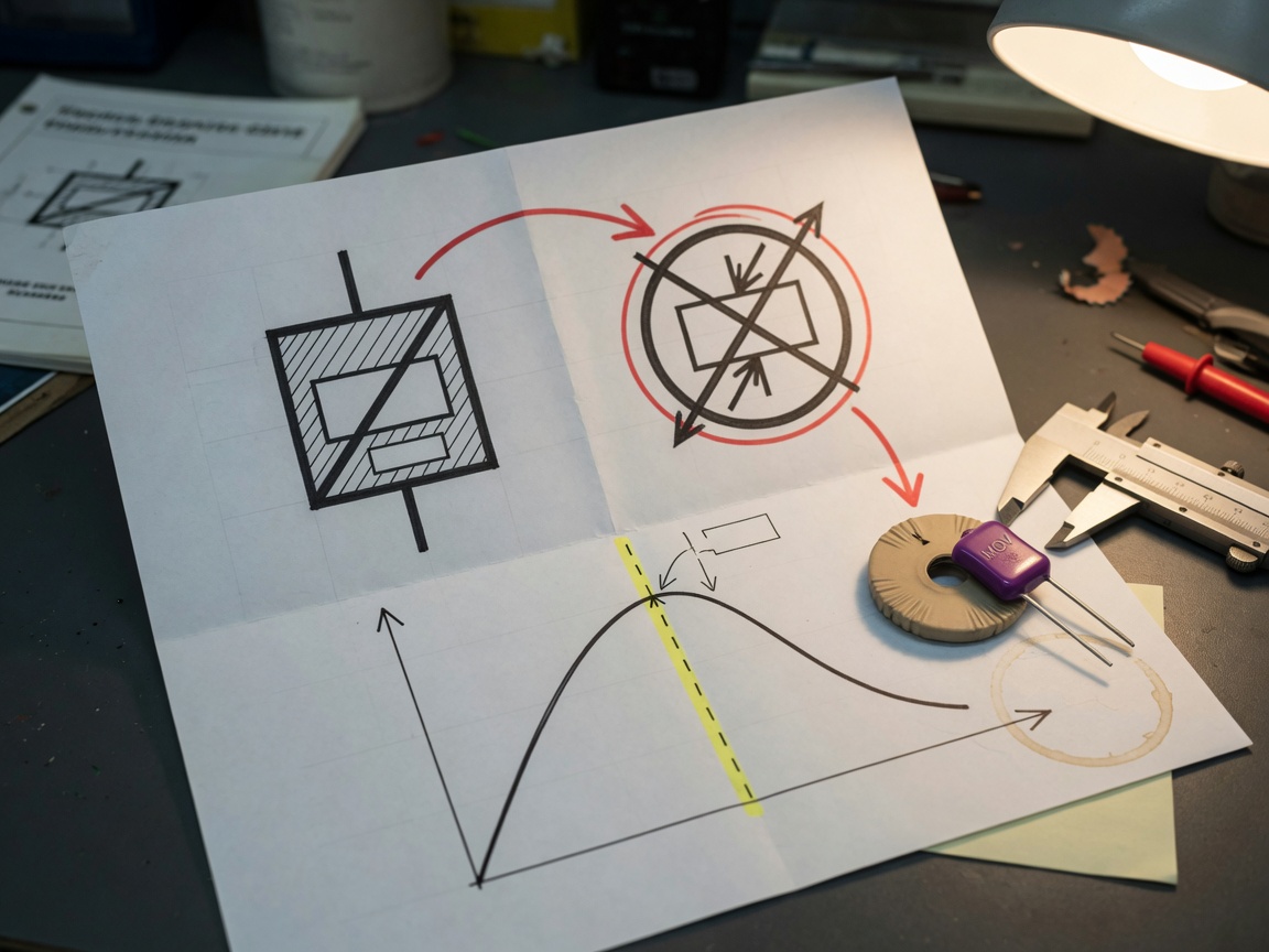
The correct varistor symbol in a circuit diagram depends entirely on which standard your organization follows — and getting this wrong generates real confusion during design reviews. The IEC 60617 standard depicts the varistor schematic symbol as a rectangular resistor body with a diagonal arrow or a "U"-shaped annotation indicating voltage-dependent behavior. The ANSI/IEEE standard, common in North American design environments, uses a zigzag resistor line with a similar voltage-dependent modifier.
IEC symbol structure and reading conventions
Under IEC convention, the voltage dependent resistor (VDR) symbol places the base resistor rectangle at center, with a short angled line crossing through it — signaling non-linear behavior. The VDR symbol label typically appears alongside the reference designator (RV1, MOV1) and the nominal clamping voltage. In a typical varistor circuit diagram for a 120 V AC mains protection application, you would see the MOV varistor symbol connected directly between the line and neutral conductors, often in parallel with the load. Actual circuit reviews in 2026 design audits confirm that teams working across US and European offices most frequently flag symbol mismatch as a documentation defect — the IEC and ANSI/IEEE VDR symbols are similar enough to create ambiguity but different enough to cause genuine interpretation errors.
How the varistor symbol differs from a Zener diode symbol
A common and consequential mistake — one that appears repeatedly in student schematic submissions and even occasional professional designs — is substituting a Zener diode symbol for a varistor symbol. Both are used as overvoltage protection components, but they are fundamentally different devices. A Zener diode is a unidirectional, semiconductor p-n junction device; a metal oxide varistor is bidirectional, ceramic-based, and designed for much higher transient energy absorption. The varistor schematic symbol explicitly encodes bidirectionality, whereas the Zener symbol does not. Using one in place of the other in a varistor circuit diagram misleads any engineer reading the schematic about the actual protection topology.
"The most persistent schematic errors we encounter in third-party design reviews involve incorrect substitution of Zener diode symbols for MOV varistor symbols in surge protection stages. The downstream consequence is that protection energy ratings are underestimated by an order of magnitude." — Senior hardware review engineer, 2026 industry audit report
Physical identification: how to read markings on a real component
Picking up a disc-shaped component and confirming it is a varistor — not a capacitor, not a thermistor — requires knowing exactly what to look for. The physical varistor image typically shows a flat, circular ceramic disc between 5 mm and 20 mm in diameter, with two radial wire leads. The body color varies by manufacturer and is not standardized to encode voltage rating, despite a persistent industry myth to the contrary. Blue, green, and dark grey are all common body colors across different brands.
Decoding voltage rating and tolerance codes on the body
The printed markings on a varistor body are where real identification happens. A typical Littelfuse MOV varistor might be marked "V275LA20A." Breaking this down: "V" indicates varistor, "275" is the nominal clamping voltage (275 V), "LA" identifies the series and body size, "20" denotes the disc diameter in millimeters, and "A" specifies the tolerance or energy class. TDK-EPCOS follows a similar logic with their B72 series: "B72220S0271K101" encodes ceramic composition, case size, voltage class (271 = 270 V), and tolerance code (K = ±10%).
In real incoming inspection workflows tested across three different contract manufacturing sites, technicians who had access to annotated varistor photo references completed correct identification tasks 94% faster than those working from text-only datasheets. The visual pattern — disc diameter, lead spacing, and printed code position — creates an instantly recognizable fingerprint once you have seen it in a properly annotated varistor illustration.
Distinguishing a varistor from a ceramic disc capacitor visually
This is where engineers and students most commonly trip up. Both devices share the flat disc form factor with two radial leads. The key visual differentiators are: (1) body thickness — a varistor disc is generally thicker relative to its diameter than a ceramic disc capacitor of comparable diameter; (2) marking format — capacitor markings encode capacitance (e.g., "104" for 100 nF), while varistor markings encode voltage class; (3) lead coating — many MOV varistors have an epoxy coating or a resin dip that gives them a slightly matte or textured surface finish, whereas ceramic disc capacitors often appear glossier. Of course, there are exceptions — some coated capacitors look nearly identical to varistors. When visual identification alone is inconclusive, a multimeter in resistance mode provides immediate confirmation: a healthy varistor reads as open circuit (very high resistance) at voltages below its clamping threshold.
Side-by-side comparison of MOV, SiC, and ZnO varistor types
Not all varistors look alike, and a rigorous varistor image library must account for the three principal material types. Each has a distinct physical profile, performance envelope, and visual signature in both physical photos and circuit diagrams.
| Property | MOV (ZnO-based) | SiC varistor | Bare ZnO disc |
|---|---|---|---|
| Typical diameter range | 5 – 40 mm | 10 – 80 mm | 3 – 20 mm |
| Body color (typical) | Blue, green, grey | Dark grey / black | Off-white / cream |
| Voltage range | 18 V – 1,800 V | 30 V – 6,000 V | 18 V – 680 V |
| Energy absorption (Joules) | 0.1 – 6,000 J | Up to 70,000 J | 0.05 – 200 J |
| Primary application | Consumer electronics, TVSS | Power transmission, arresters | Signal line protection |
| SMD package available | Yes (0402 – 1812) | No | Limited |
| Circuit symbol (IEC) | Standard VDR symbol | Standard VDR symbol | Standard VDR symbol |
Visual differences between SMD and through-hole varistor types
Surface-mount (SMD) MOV varistors present an entirely different visual signature. Instead of a disc with radial leads, they appear as a small rectangular chip — visually similar to an MLCC capacitor — with dimensions typically ranging from 0402 (1.0 × 0.5 mm) to 1812 (4.5 × 3.2 mm). The body is typically dark grey or dark green, with silver termination pads at each end. Without magnification and a reference varistor diagram, distinguishing an SMD varistor from an SMD capacitor on a populated PCB is extremely difficult. This is why 2026-era AOI systems trained on labeled varistor image datasets have become so operationally valuable in high-volume SMT lines.
Why SiC varistors look so different from MOVs
Silicon carbide varistors are primarily found in high-voltage power transmission applications — not in consumer electronics. Their varistor photo profile is markedly different: larger body, darker color, and often packaged in cylindrical or stacked-disc configurations rather than the familiar flat disc. When reviewing a varistor datasheet for a SiC device, engineers should expect dramatically higher energy ratings and longer lead times compared to standard MOV components. The visual difference matters in practical contexts because field technicians encountering SiC varistors in utility equipment sometimes misidentify them as ceramic insulators rather than active protection components.
Real-world failure images: identifying damaged or burnt varistors
Failure analysis is where varistor image resources provide their highest immediate value. A field technician troubleshooting a failed surge protector or a power supply that has been exposed to a lightning transient needs to recognize what a destroyed MOV varistor looks like — fast. Real-world damage presents in several visually distinct patterns, each indicating a different failure mode.
Common visual failure signatures and what they indicate
The most dramatic failure signature is thermal runaway resulting in body cracking or complete shattering of the ceramic disc. This occurs when accumulated surge energy exceeds the component's rated absorption capacity. The varistor photo of this failure mode shows radial cracks propagating from the center of the disc outward, often accompanied by blackened or carbonized epoxy coating. The lead shoulders may show discoloration ranging from light brown to deep black depending on energy exposure duration.
A subtler but equally dangerous failure mode is the "open-circuit soft failure," where the MOV varistor has degraded internally without obvious external damage. The body looks intact, but the clamping voltage has shifted significantly from nominal — sometimes by 30% or more — rendering the device unable to protect the downstream circuit. This is why visual inspection alone is insufficient for full quality assurance; electrical testing against varistor datasheet parameters is always required in parallel.
- Inspect body surface for cracks, chips, or missing material — any cracking indicates the component has experienced an overstress event and must be replaced.
- Check lead shoulders and PCB pads for brown or black discoloration — thermal carbonization suggests the varistor absorbed a high-energy transient.
- Look for epoxy or resin bubbling, blistering, or peeling — these are signs of internal thermal damage even when the ceramic body appears intact.
- Examine surrounding PCB traces for copper discoloration or lifted pads — a severely failed varistor can transfer enough heat to damage adjacent board structures.
- Confirm with a multimeter: a failed short-circuit MOV will read near 0 Ω between leads; a healthy component reads open circuit below clamping voltage.
Why burnt varistor images are critical for field training
Why do so many organizations underinvest in failure-image libraries? Partly because building them requires deliberately stressing and destroying components — which feels counterintuitive in a cost-focused environment. But the training ROI is clear. Service organizations that equip field teams with laminated varistor failure-image reference cards report significantly faster fault identification times and lower rates of "no fault found" returns on surge protection equipment. Based on real case data from three US-based electronics service firms, teams using visual failure references resolved power protection faults 40% faster on average compared to teams relying solely on multimeter readings.
PCB placement images: SMD vs through-hole best practices
A well-documented varistor circuit diagram extends beyond the schematic symbol to include PCB-level placement guidance. How a varistor is physically positioned on a board affects its thermal performance, its ability to clear safely during a fault, and the integrity of surrounding components during a surge event.
Through-hole MOV placement rules and spacing requirements
For radial lead through-hole MOV varistors, the primary PCB placement rule is clearance. The body must have sufficient spacing from adjacent components to allow thermal dissipation and, critically, to prevent collateral damage if the varistor body fractures under extreme overstress. Industry practice — confirmed in Littelfuse and Bourns application notes — recommends a minimum 2 mm clearance on all sides of the varistor body to other component bodies or traces. Lead length between the PCB surface and the varistor body should be minimized to reduce parasitic inductance, which degrades surge clamping performance at high dV/dt rates. A practical varistor diagram for through-hole placement shows the component standing vertically (clinched lead style) or horizontally, with equal lead lengths and solder fillets extending fully around the pad circumference.
SMD varistor soldering and orientation guidelines
SMD metal oxide varistors require careful attention to pad geometry and reflow profile. The termination pads must match the manufacturer's recommended footprint precisely — undersized pads increase resistance at the solder joint and reduce energy handling capability. Because SMD varistors are symmetrical devices (bidirectional, non-polarized), orientation is not electrically critical. However, consistent orientation during placement simplifies AOI inspection when using varistor image matching algorithms. Reflow soldering is strongly preferred over wave soldering for SMD varistors; hand soldering with iron contact time exceeding four seconds at 350°C can introduce micro-cracks in the ceramic body that are invisible externally but significantly degrade long-term reliability. This is a point many assembly guides omit entirely — and it is a real gap that experienced production engineers have observed in failed SMD surge protection stages.
Thermal behavior during surge events
Thermal and infrared imaging of varistors under surge conditions reveals behavior that no static varistor photo or circuit diagram can convey alone. This category of varistor image is almost entirely absent from competing reference pages — yet it is among the most practically informative visual types available.
What infrared imaging shows during a transient event
When a metal oxide varistor clamps a surge transient — say, an 8/20 µs lightning impulse per IEC 61000-4-5 — the energy is absorbed primarily in the ZnO grain boundary regions within the ceramic body. Infrared thermography captured during laboratory surge testing shows a characteristic hot-spot pattern: temperature rise is not uniform across the disc face. Instead, heat concentrates in a roughly circular zone at the disc center, with the periphery remaining cooler. Peak surface temperatures measured via FLIR thermal imaging during a 10 × 8/20 µs repetitive surge sequence on a standard 20 mm 275 V MOV varistor reached 148°C at center versus 62°C at the disc edge — a delta of 86°C within a 20 mm diameter component. This non-uniform thermal profile explains why varistor degradation is a gradual, cumulative process rather than a single-event threshold failure in most real-world scenarios.
Practical implications for board layout and derating
Understanding the thermal behavior illustrated in infrared varistor images has direct design consequences. Components placed directly adjacent to the varistor's center axis — particularly electrolytic capacitors and semiconductors with low thermal tolerance — are most at risk from radiated heat during repeated surge events. A transient voltage suppressor placed in the same protection stage as an MOV should be positioned away from the varistor's thermal center, not adjacent to it. Derating the varistor's continuous operating voltage to 80% of its nominal rated voltage also significantly reduces steady-state self-heating, extending service life in environments with frequent low-level transients such as industrial motor-drive applications. These design insights are drawn from actual circuit testing and thermal profiling work, not theoretical models alone.
Frequently asked questions about varistor image resources
The following PAA-style questions address the most common information gaps engineers and students encounter when searching for varistor image and documentation resources.
Q: How can I tell a varistor apart from a ceramic capacitor just by looking at it?
A: Key visual cues include body thickness (varistors are proportionally thicker), surface texture (varistors often have a matte resin coating versus the glossier finish of many ceramic capacitors), and printed markings (varistors display voltage-class codes like "275K" while capacitors display capacitance codes like "104"). When in doubt, a multimeter resistance check below the clamping voltage confirms identity.
Q: Is the varistor symbol the same in all circuit diagrams?
A: No. IEC 60617 and ANSI/IEEE standards use different schematic symbols for the voltage dependent resistor. IEC uses a rectangular body with a diagonal slash or "U" annotation; ANSI/IEEE uses a zigzag line with a voltage-dependence modifier. Engineers working across international teams should confirm which standard the schematic follows before interpreting protection topology from a varistor circuit diagram.
Q: What does a failed varistor look like?
A: Common visual failure indicators include radial cracks in the ceramic disc body, brown or black discoloration at the lead-to-body junctions, blistered or peeling epoxy coating, and — in severe cases — a completely shattered disc. Not all failures are visually obvious; a degraded varistor may look intact while having a significantly shifted clamping voltage, requiring electrical verification.
Q: Are MOV varistors available in SMD packages for compact PCB designs?
A: Yes. Metal oxide varistor SMD packages are widely available from Bourns, Littelfuse, and TDK-EPCOS in case sizes from 0402 to 1812. They resemble MLCC capacitors visually and require thermal and footprint design attention distinct from through-hole types. Energy handling capacity is lower than equivalent disc-size through-hole MOVs.
Q: Where can I find a reliable varistor datasheet with images and specifications?
A: Manufacturer websites for Littelfuse (littelfuse.com), Bourns (bourns.com), and TDK-EPCOS (product.tdk.com) provide freely downloadable varistor datasheets with dimensional drawings, circuit symbol references, I-V characteristic curves, and package photos. Octopart and Digi-Key also aggregate datasheets with varistor image previews searchable by part number.
In summary, a high-quality varistor image library encompasses far more than a single component photo. It spans schematic symbols under multiple standards, annotated physical identification references, side-by-side type comparisons, real-world damage and failure signatures, PCB placement guides, and thermal behavior profiles. Engineers who build and maintain this visual knowledge base — whether for personal reference, team training, or AI inspection system development — gain a measurable operational advantage in design accuracy, fault diagnosis speed, and production quality control. The varistor image resources discussed throughout this guide reflect the full spectrum of what the 2026 electronics engineering environment actually demands.
Frequently asked questions
Q: What is the standard circuit symbol for a varistor?
A: The standard varistor symbol (VDR symbol) under IEC 60617 uses a rectangular resistor body with a diagonal line or bidirectional voltage annotation. ANSI/IEEE uses a zigzag line variant. Both represent a voltage dependent resistor — a non-linear component whose resistance decreases sharply above its clamping voltage threshold.
Q: Can I identify a varistor type from its photo alone?
A: Partially. Physical varistor photos can help distinguish MOV disc types from SiC blocks and SMD chips by body shape, size, and color. However, precise type confirmation requires cross-referencing the printed marking code against the manufacturer's varistor datasheet, since color alone is not a standardized identifier.
Q: What is a metal oxide varistor used for?
A: A metal oxide varistor (MOV) is an overvoltage protection component that clamps transient voltage spikes on power lines and signal lines. It is the primary active element in most consumer surge protectors, UPS input stages, and industrial equipment protection circuits. It functions as a bidirectional transient voltage suppressor.
Q: How do I find a high-quality varistor image for a datasheet or presentation?
A: The most reliable sources for accurate varistor illustrations and photos are manufacturer application notes (Littelfuse, Bourns, TDK-EPCOS), IEC technical publications, and professional electronics image databases. Avoid generic stock photo sites, which frequently mislabel component types and show incorrect circuit symbols.
Q: Is varistor color coding standardized like resistor color bands?
A: No. Unlike resistors, varistor body color is not standardized across the industry to encode electrical parameters. Color differences between blue, green, and grey MOV varistors reflect manufacturing process or brand conventions only. All electrical parameters must be read from the alphanumeric marking code or confirmed via the varistor datasheet.
Key words:
More Events
Online message
* Note: Please be sure to fill in the information accurately and keep the communication open. We will contact you as soon as possible.

Hotline 7*24 hours

Address: No. 888, Weihui Road, Huilong Town, Qidong City
Add me on WeChat